There are many different types of DC/DC converters, each with a unique mode of operation. The one proposed in this article involves the analysis of a DC/DC boost converter operating in Class E with dual-frequency signal drive. This solution allows the output power to be adjusted if the load should change. One of the most important features of the circuit is that it can ensure very high efficiency under all operating conditions. The boost converter examined in this article allows the output DC voltage to be higher than the input DC voltage with maximum efficiency.
Fixed load and variable load in Class E
When a Class E converter is designed for a precisely valued load, it has no control to adjust the output parameters. The output signal characteristics are fixed and always operate under the same conditions. If, on the other hand, different loads are to be used, a series of controls must be arranged to perfectly adjust the output signal. When the output impedance changes, the circuit’s modes of operation change, as do the waveforms of the signals.
Efficiency is not always constant and varies, depending on the type of load applied. With Class E converters, it is possible to obtain special waveforms that pass through zero before the instant of switching. In this way, the switching losses are very low. In Class E converters, the switching frequency can be greatly increased compared with conventional converters, even by a factor of 50, allowing high efficiencies to be achieved.
Due to this aspect, circuit sizes can be kept small, resulting in a significant reduction in weight, footprint and final cost. The EMI aspect is also dramatically reduced. In normal switching, power-electronic switches interrupt the current within very short moments, which causes great stress to the electronic components. They must endure high voltages and high currents simultaneously, causing great power dissipation and stress, which results in power losses and low efficiencies.
By adopting resonant circuits in converters, waveforms can be shaped to create zero-voltage–switching and zero-current–switching conditions. By reducing power dissipation (ideally to zero), increasing switching frequency and eliminating transient spikes, overall system efficiency is increased for very low EMI.
Dual-frequency control in boost converters
Class E converters usually work for a single load case because they are designed to operate only under a specific operating condition. Normally, they provide for a specific type of load, and in this case, the converter operates at maximum efficiency, with only one optimum operating point. By changing the load, the waveforms of the circuit change, and therefore, optimal operation is no longer guaranteed. A change of load results in a drastic reduction in system efficiency.
To solve these problems, it is possible to modulate the output current using dual-frequency control, with which an optimal operating point is always guaranteed, and the efficiency of the entire system is maintained at very high values. In switching converters, the most critical components are the inductors. Fortunately, in this circuit implementation, these components do not have to be replaced, and the optimal operating point can be equally achieved by adopting two different switching frequencies. Speci energy c precautions must be taken when implementing a dual-frequency Class E boost converter, as shown in Figure 1.

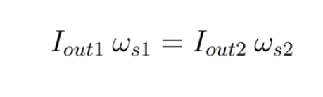
The same inductors can be used in this circuit without having to replace them. Instead, the optimal operating point at both frequencies is obtained simply by changing the value of the capacitors connected in parallel with the electronic switches. Maximum efficiency is obtained only if the product of the output current and the switching frequency of the transistor remains constant. This solution is derived from the single-frequency boost, in which there are no electronic switches that alternately connect and disconnect the additional pair of capacitors.
It is easy to see that when such switching devices are in conduction, they allow additional capacitors to be connected in parallel to increase the capacitance to those already existing in the scheme. Another condition required by the circuit is that the product must be kept constant to protect maximum efficiency at the two switching frequencies:
Circuit operation
Unlike the scheme with only one operating frequency, this one has two switches in series, with the two capacitors labeled Cinv1 and Crec1, allowing the total capacitance to be changed. If the switches are closed, the capacitances of Cinv1 and Crec1 are added to the Cinv2 and Crec2 capacitors, respectively. In this case, the converter works at a lower frequency. On the other hand, if the additional capacitances are disconnected, the converter works at the higher frequency. Note that the additional switches are two MOS transistors. However, the one in series with Cinv2 is N-channel, while the one in series with Crec2 is P-channel. The converter operates at one of two switching frequencies, depending on the input voltage and load conditions, in the following two ways:
● If the input voltage is high, or the load is light, the circuit adopts the higher switching frequency so that the on-off transition losses and conduction losses produced by the resonant inductor can be reduced.
● When the voltage is low, or the load possesses low impedance, the circuit adopts the lowest switching frequency.
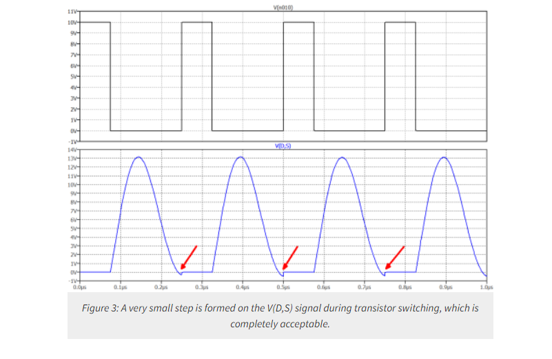
At the design stage, the input and output operating voltages, at which the converter is to work, must be chosen. Likewise, the designer must choose the two maximum powers dissipated by the load, at the two frequencies. With these, the currents of the two branches, INV and REC, can be easily calculated. The determination of the inductive components is extremely delicate, as it must also consider the two frequencies involved. The graphs in Figure 2 show the waveforms of the voltage between the drain and source of the electronic switch V(D,S) and the voltage between the cathode and anode of the diode V(K,A).
The following steps should be followed to obtain two good working conditions at the two chosen frequencies. Usually, it is better to prefer one frequency twice as high as the other:
● Choose the input voltage and the output voltage.
● Determine the maximum relative powers at the two frequencies involved.
● Calculate the relative currents.
● Choose the inductors and determine the respective q-values, at the two frequencies.
● Calculate the switching losses.
● Optimize the results by slightly adjusting the component values.
The first sizing of the components is done at a given frequency; the second sizing is done, however, at twice the frequency. The switching losses are again calculated, and finally, further optimization is performed. This is far from a simple procedure.

A well-designed circuit results in very high efficiency, and the peak values of the two voltages examined earlier are not critical and are supported by most devices on the market. The value of the average output current is equivalent to the average current of IREC. Parasitic resistive components in series with the reactive components (capacitors and inductors) must be considered when designing the circuit. These parasitic resistances are subject to change in relation to frequency; indeed, they are more relevant at high frequencies. To make a single circuit work at the two frequencies, it is necessary to combine two equivalent designs to implement a Class E boost converter that can work at the two frequencies.
As mentioned before, if the two switching devices in series with the capacitors Cinv1 and Crec1 are open, the circuit can operate at the higher frequency. Conversely, if these electronic switches are closed, the circuit operates at a lower frequency. At such frequencies, therefore, the presence of parasitic resistances varying according to the frequency itself is inevitable. Such reactances will be minimal as far as capacitors are concerned, while for inductors, they may reach important values due to their low Q.
In the graph in Figure 3, there is a small step on the oscillogram related to the V(D,S) voltage, just at the instant when the electronic device is turned on and goes into conduction. This step cannot be eliminated altogether and results in a very small increase in the power dissipated in switching, which is completely acceptable and insignificant.
Conclusion
Experimental results show that, with this dual-frequency methodology, the conversion efficiency improves by at least 6% to 7%. By performing a good analysis and design, the circuits behave as planned, achieving their intended goals. It is interesting to compare the voltage waveforms at the ends of the MOSFET and diode, at the two switching frequencies, to verify the efficiency of the system. It is useful, too, to analyze the currents transiting the LINV and LREC inductors.
The oscillograms in Figure 4 show, respectively, the activation pulse of the electronic switch and its two signals at the ends of the two semiconductor components (the first two oscillograms above) at the base frequency. The other two oscillograms (bottom) show, respectively, the activation pulse of the electronic switch and its two signals at the ends of the two semiconductor components, at the double frequency. The second mode of operation uses twice the frequency and half the current on the load. These results, at such high frequencies, could not normally be achieved with conventional solutions.
Class DC/DC converters are extremely complex and critical, but they provide enormous benefits by allowing loads of varying nature and impedance to be driven. With special arrangements and substantial circuit modifications, and with an exponential increase in system complexity, a DC/DC converter can also be implemented for three types of loads.
About US
Heisener Electronic is a famous international One Stop Purchasing Service Provider of Electronic Components. Based on the concept of Customer-orientation and Innovation, a good process control system, professional management team, advanced inventory management technology, we can provide one-stop electronic component supporting services that Heisener is the preferred partner for all the enterprises and research institutions.