The pursuit of high efficiency and high power applications continue to develop towards higher power density and cost optimization, and also create sustainable value for electric vehicles and other industries. To address these challenges, Infineon Technologies announced that QDPAK and DDPAK Top cooled (TSC) packages for its high-voltage MOSFET devices have been successfully registered as JEDEC standard. This move not only further strengthens Infineon's goal to extend the standard package design and shape of the TSC package to a wide range of new designs, but also gives Oems more flexibility and advantage to create differentiated products in the market and raise power density to even higher levels to support a variety of applications.

"As a solutions provider, Infineon continues to make an impact on the semiconductor industry through innovative packaging technologies and processes," said Ralf Otremba, chief engineer of High voltage packaging at Infineon Technologies. Our advanced top-cooled packages offer significant benefits at the device and system levels, meeting the challenging requirements of cutting-edge, high-power designs. "Standardization of package shapes ensures pin compatibility across vendor designs -- one of the key design considerations for Oems in high-voltage applications -- eliminating the need for this effort."
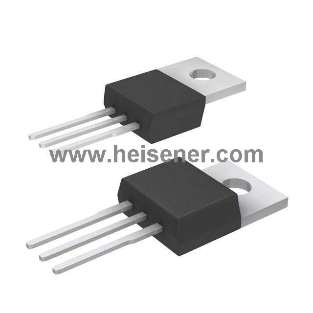
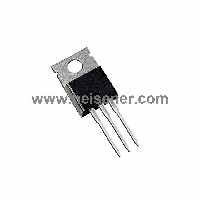
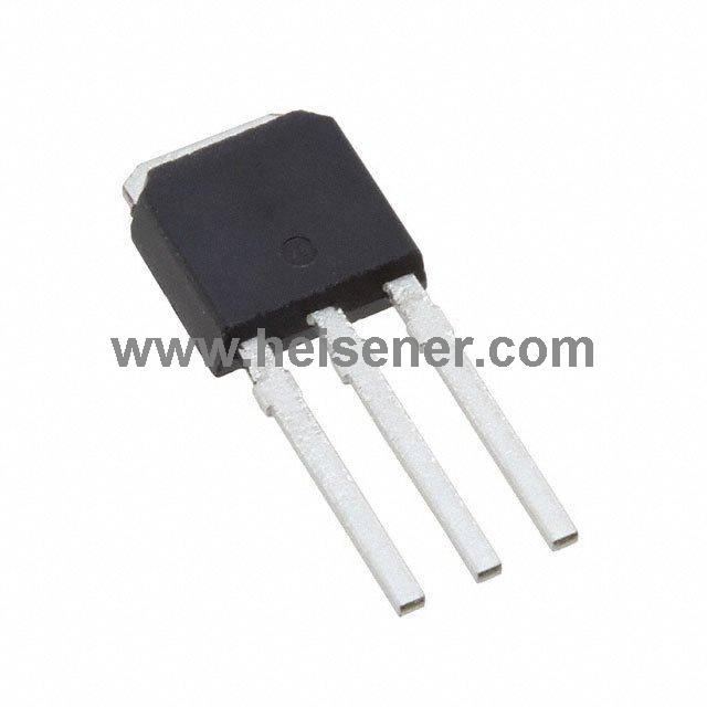
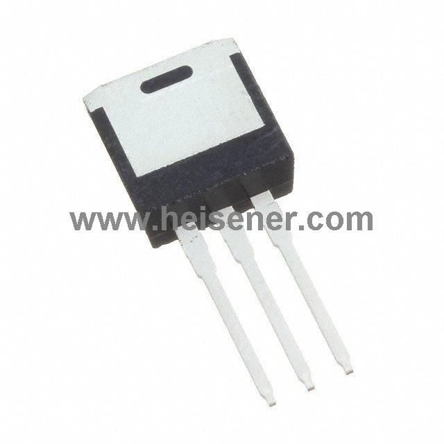
For more than half a century, the JEDEC organization has led the global microelectronics industry in a wide range of technologies, including the development of open standards for packaging and publications. JEDEC incorporates a wide range of semiconductor packages, such as TO220 and TO247 through-hole devices (THDS), which have seen widespread adoption over the past few decades and are still available as design options for new on-board charger (OBC) designs, high-voltage (HV) and low-voltage (LV) DC-DC converters.
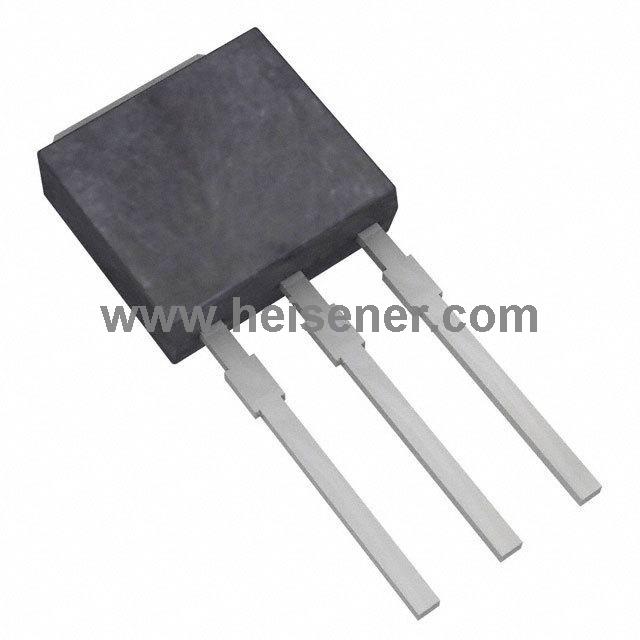
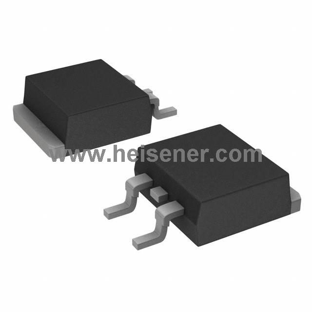
The successful registration of the QDPAK and DDPAK Surface Mount (SMD)TSC package designs marks the beginning of a new era in packaging appearance and will drive wider adoption of TSC technology to replace the TO247 and TO220. With this technology advantage and the MO-354 standard, the new Jedec-registered package family will be a key driver in the transition to next-generation top cooling designs for high-pressure industrial and automotive applications.

To assist customers with the design transition between TO220 and TO247 THD devices, Infineon has introduced QDPAK and DDPAK SMD devices that provide equal heat dissipation and better electrical performance. The QDPAK and DDPAK SMD TSC packages for HV and LV devices come in a 2.3mm standard height, allowing developers to design complete applications using all SMD TSC devices of the same height, such as OBC and DC-DC conversion. This package not only benefits the design, but also reduces the cost of the cooling system compared to existing solutions that require the use of 3D cooling systems.
In addition, the TSC package reduces thermal resistance by up to 35% compared to standard bottom cooling (BSC). TSC package takes full advantage of the double-sided PCB, providing better board space utilization and at least twice the power density. Since the thermal resistance of the package pins is much higher than that of the exposed package top, the thermal management of the package can also be improved by the pyrolytic coupling of the substrate. The improved cooling efficiency eliminates the need to stack different boards. A single FR4 is sufficient for all components, eliminating the need to combine FR4 with IMS and requiring fewer connections. Each of these features contributes to the overall bill of Materials (BOM), which ultimately reduces the overall system cost.

In addition to improved heat dissipation and power capabilities, TSC technology also provides a better power loop design because the driver configuration can be located very close to the power switch and is therefore more stable. The low spurious inductance of the driver switching loop can reduce the parasitic effect of the loop, so the grid oscillation is less, the efficiency is higher, and the risk of failure is less.